

+91 9909953035
Amorphous | Polycrystalline | Single Crystal |
|---|---|---|
Random, disordered atomic arrangement | Made of many small crystal grains | Uniform, continuous atomic lattice |
No long-range structural order | Each grain has a different orientation | No grain boundaries |
Irregular and non-uniform | Grain boundaries exist | High structural integrity and uniformity |
📌 Examples: Glass, Plastic, Amorphous carbon | 📌 Examples: Metals, Ceramics, Polycrystalline diamond | 📌 Examples: Natural diamond, Silicon wafers, Sapphire |
Crystalline materials form the backbone of modern electronics, photonics, and structural applications. From the internal atomic arrangement to specialized materials like wide bandgap semiconductors, understanding these fundamental concepts unlocks innovations in semiconductors, solar cells, and nanotechnology.
Crystals are solids with atoms arranged in a highly ordered, repeating 3D lattice. This atomic arrangement defines the physical, electrical, and mechanical properties of the material.
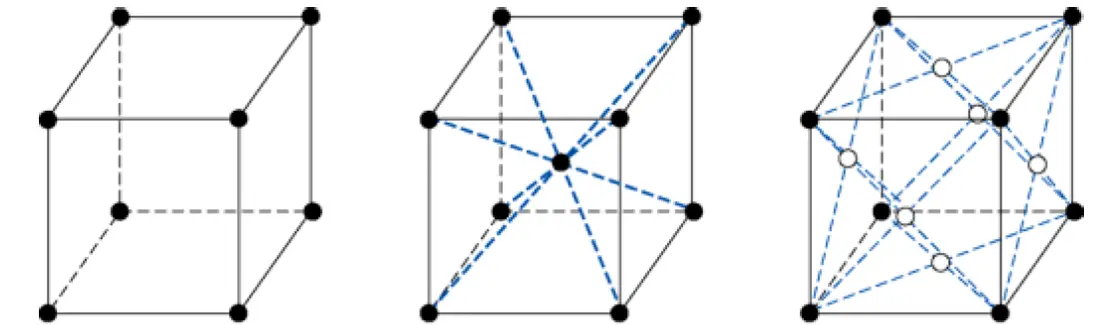
Property | Simple Cubic (SC) | Body-Centered Cubic (BCC) | Face-Centered Cubic (FCC) |
|---|---|---|---|
Atomic Positioning | Atoms at each corner of the cube | Atoms at corners and one at the center | Atoms at corners and centers of each cube face |
Packing Efficiency | ~52% (Low) | ~68% | ~74% (High) |
Occurrence | Rare in nature (inefficient packing) | Common in metals like Iron (below 912°C), Chromium | Common in ductile metals like Copper, Gold, Aluminum |
Mechanical Properties | Brittle, low efficiency | Strong but less ductile | Highly ductile, good slip planes for deformation |
Examples | Theoretical model, Polonium | Iron, Chromium, Tungsten | Aluminum, Copper, Gold, Silver |
Crystal planes are specific orientations of atoms within a crystal lattice, often denoted by Miller Indices like {100}, {110}, {111}. These planes are crucial in determining material behavior.
Why Crystal Planes Matter:
Examples:
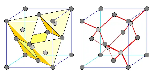
Diamond uses a diamond cubic structure, a variation of the FCC lattice with each atom covalently bonded to four others in a tetrahedral geometry.
🔹 Diamond Properties:
Structurally stable under extreme conditions
WBG semiconductors have a larger energy gap (Eg) between the valence and conduction bands, making them ideal for high-power, high-frequency, and high-temperature applications.
Bandgap Comparison:
Material | Bandgap (Eg in eV) |
|---|---|
Germanium (Ge) | 0.7 |
Silicon (Si) | 1.1 |
GaAs | 1.4 |
SiC | 3.3 |
ZnO | 3.4 |
GaN | 3.4 |
Diamond (C) | 5.5 |